


What are the Sources of Wastewater Generated during the PCB Manufacturing Process?
Electroplating is one of the world's top three polluting industries. With industrialization advancing, the discharge of electroplating wastewater has increased significantly. Electroplating wastewater contains acids, alkalis, heavy metal ions, and other toxic substances. To address environmental concerns, more electroplating parks and enterprises are adopting zero liquid discharge (ZLD) technologies, achieving water recycling. In ZLD systems, evaporators are essential and determine whether wastewater can be fully recycled.
PCB (Printed Circuit Board), known as the “mother of electronics,” involves numerous chemical plating and electroplating processes, producing wastewater far more complex than conventional electroplating. So, where does PCB wastewater come from, and how can it be effectively treated? Let’s explore.
1. PCB Industry: High Water Usage and Environmental Challenges
Printed circuit boards are widely used in computers, communications, consumer electronics, industrial control, medical devices, defense, semiconductors, and automotive applications. China is now the largest PCB manufacturer globally, which brings significant environmental challenges.
According to statistics, China’s PCB wastewater volume increased from 278–336 million tons in 2007 to about 600 million tons in 2010, and the number continues to rise. Water consumption mainly depends on the number of PCB layers—the more layers, the higher the water usage. PCB wastewater contains toxic heavy metals (Cu²⁺, Ni²⁺), cyanides (CN⁻), organics, NH₃-N, TN, TP, and other hazardous pollutants.
2. Sources of PCB Wastewater
Understanding PCB wastewater requires looking at each production process:
• PCB production wastewater mainly comes from:
Grinding, board washing, developing, etching, micro-etching, stripping, black/brown oxide, deburring, glue removal, through-hole plating, copper plating, tin plating, tin stripping, solder mask, nickel plating, gold plating, pre/post tin treatment, etc.
Different processes produce different pollutants, making classification and separate treatment essential.
9 Main Sources of PCB Wastewater:
| Wastewater Type | Processes | Pollutants | Notes |
|---|---|---|---|
| General Cleaning Wastewater | Grinding, washing, micro-etching, developing, copper plating cleaning | Copper powder, ash, copper ions, minor organics | Largest portion (~50–70% of total volume), low concentration but large quantity |
| Complexed Copper Wastewater | Alkaline etching cleaning | Copper ions (complexed), ammonia nitrogen, total nitrogen | Stable copper-ammonia complexes are hard to remove via conventional precipitation |
| Chemical Copper Deposition Wastewater | Cleaning after chemical copper deposition | Complexed copper ions, organics (e.g., formaldehyde, EDTA) | — |
| Chemical Nickel Plating Wastewater | Chemical nickel plating cleaning | Nickel ions (complexed), phosphates, ammonia, organics | High environmental risk; strict discharge standards |
| Electroplated Nickel Wastewater | Electrolytic nickel plating cleaning | Nickel ions, organics | Easier to treat than complexed nickel |
| Cyanide-Containing Wastewater | Gold plating, chemical gold/silver deposition cleaning | Cyanides (toxic) | Pre-treatment required (cyanide destruction) before entering main wastewater treatment |
| Ink Wastewater | Developing, stripping, screen printing cleaning | Photoresist residues, solder mask residues, high COD (>10,000 mg/L) | — |
| Mixed Wastewater | Pre-treated wastewater from all above sources + degreasing, oil removal | Organics, heavy metals | Main target of wastewater treatment |
| Concentrated Wastes | Etching, tin stripping, chemical nickel mother liquor, high-concentration organics | — | High concentration; treated as hazardous waste or recovered for reuse |
3. Treatment Challenges and Solutions
Core Principle: Classification + Pre-Treatment
PCB wastewater contains variable metal ions and organics in complex forms. The standard approach:
• Cyanide-containing water → two-stage cyanide destruction
• Nickel-containing water → separate pre-treatment
•Ink wastewater → acid precipitation or co-precipitation to reduce COD
• Complexed copper water → complex-breaking or resin adsorption
Pre-treated wastewater enters the integrated treatment system (physical-chemical + biological).
Key to Zero Discharge: Evaporators
Evaporators are critical for zero liquid discharge. WTEYA’s ZLD system treats membrane concentrates efficiently:
• No secondary pollution
• Water quality meets reuse standards
• Reduces water costs and hazardous waste disposal
MVR Evaporators are most effective for PCB concentrated waste, recovering water for production and leaving salts as residual hazardous waste. Systems like “electrolytic copper recovery + MVR evaporator + gas treatment” achieve zero discharge while recovering valuable metals.
4. Conclusion
PCB wastewater treatment requires:
• Classification: Accurate separation of waste streams
• Pre-treatment: Effective removal of complex metals and organics
• Evaporation and crystallization: Efficient zero discharge
A proper treatment strategy not only protects the environment but also allows water reuse and metal recovery, reducing operational costs. WTEYA’s MVR and mother liquor drying solutions provide a mature, energy-efficient, and reliable approach for PCB wastewater management.
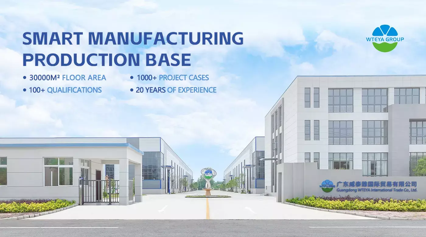
Why Partner with WTEYA?
• Nearly 20 years of industry experience
• Trusted by global leaders including Foxconn, Huawei, Ganfeng Lithium, Ronbay Technology
• 100+ success cases worldwide
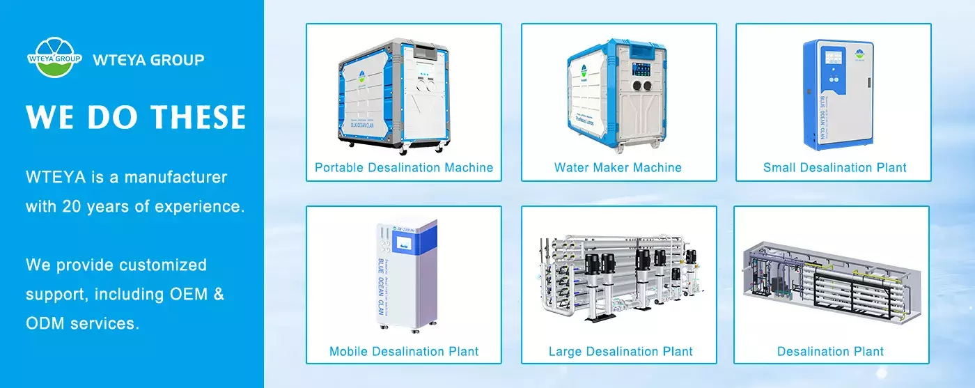
• OEM & ODM customization available
Become a WTEYA Distributor!
We are expanding global partnerships:
• Preferential policies
• Professional training
• Full technical support
Let us help you achieve exceptional water quality and operational sustainability!
📲 WhatsApp: +86-1800 2840 855
📧 Email: info@wteya.com
🌐 Website: www.wteya.com